Product Details
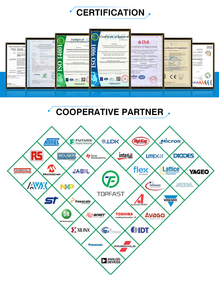
We focus on the field of pcb more than 20+ years,and we have ISO9001 quality management system certification,rosh,ISO14001 environmental management system certification,TS16949 automobile quality management system certification and other certification.
| Item | Rigid PCB |
| Max Layer | 60L |
| Inner Layer Min Trace/Space | 3/3mil |
| Out Layer Min Trace/Space | 3/3mil |
| Inner Layer Max Copper | 6oz |
| Out Layer Max Copper | 6oz |
| Min Mechanical Drilling | 0.15mm |
| Min Laser Drilling | 0.1mm |
| Aspect Ratio(Mechanical Drilling) | 20:1 |
| Aspect Ratio(Laser Drilling) | 1:1 |
| Press Fit Hole Ttolerance | ±0.05mm |
| PTH Tolerance | ±0.075mm |
| NPTH Tolerance | ±0.05mm |
| Countersink Tolerance | ±0.15mm |
| Board Thickness | 0.4-8mm |
| Board Thickness Tolerance(<1.0mm) | ±0.1mm |
| Board Thickness Tolerance(≥1.0mm) | ±10% |
| Impedance Tolerance | Single-Ended:±5Ω(≤50Ω),±7%(>50Ω) |
| Differential:±5Ω(≤50Ω),±7%(>50Ω) | |
| Min Board Size | 10*10mm |
| Max Board Size | 22.5*30inch |
| Contour Tolerance | ±0.1mm |
| Min BGA | 7mil |
| Min SMT | 7*10mil |
| Surface Treatment | ENIG,Gold Finger,Immersion Silver,Immersion Tin,HASL(LF),OSP,ENEPIG,Flash Gold;Hard gold plating |
| Solder Mask | Green,Black,Blue,Red,Matt Green |
| Min Solder Mask Clearance | 1.5mil |
| Min Solder Mask Dam | 3mil |
| Legend | White,Black,Red,Yellow |
| Min Legend Width/Height | 4/23mil |
| Strain Fillet Width | / |
| Bow & Twist | 0.3% |
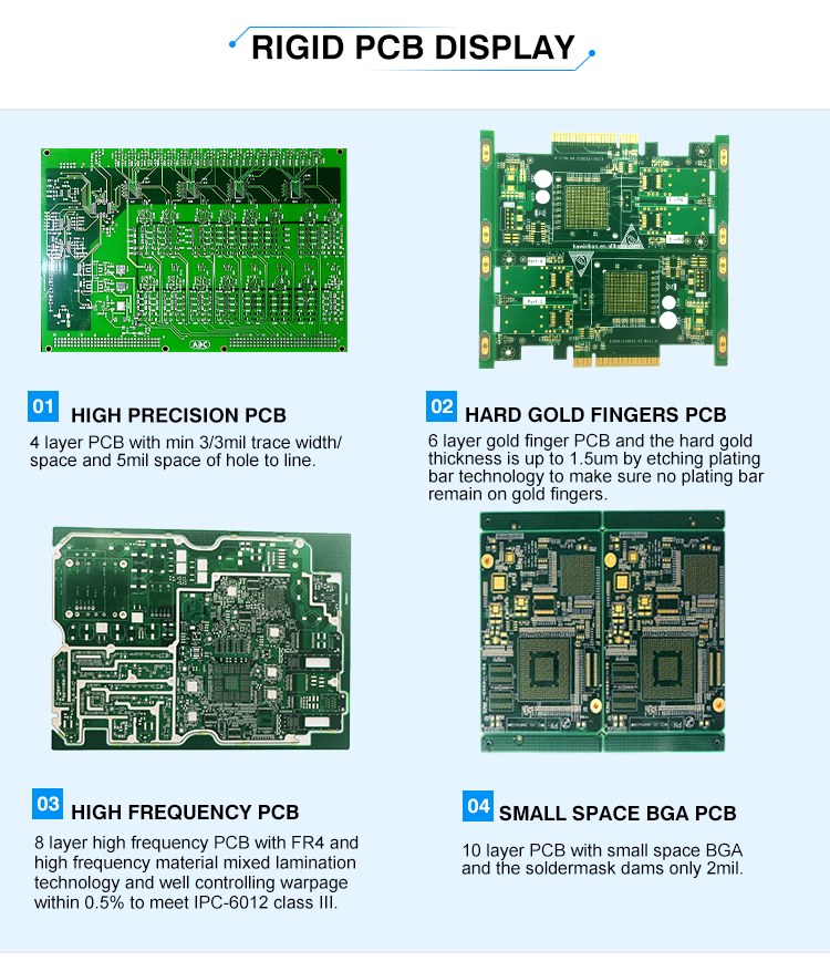
Rigid pcb also includes high precision pcb,hard gold fingers pcb,high frequency pcb,small saplce bga pcb.
The high precision pcb:4 layer pcb with min 3/3mil trace wideth/space and 5 mil space of hole to line.
Hard gold fingers pcb: 6 layer gold finger pcb and the hard gold thickness is up to 1.5um by etching plating bar technology
to make sure no plating bar remain on gold fingers.
High frequency pcb:8 layer high frequency pcb with fr4 and high frequency material mixed lamination technology and well
controlling warpage within 0.5% to meet IPC-6012 Class Ⅲ.
Application of PCB

PCB application in consumer electronics,Aerospace,Telecom communication,Military&Defense,Industrial control,automotive industry.
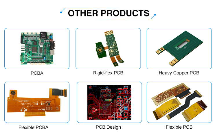
We also with pcba,rigid-flex pcb,heavy copper pcb,flexible pcba,pcb design,flexible pcb service.

Why choose us?
1.One-stop pcb pcba Service
We can help you with one-stop service.To support you with the whole processfrom function research and development,product design discussion, PCB manufacturing,component procurement to PCB assembly.
2.Advanced Equipment
There are more than 385 equipment,mainly imported from Germany, Japanand Taiwan. Such as LDl automatic ex-posure machine, automatic plating line,laser drilling machine,automatic testingmachine, automatic V-cutting machineand other advanced equipment.
3.Advanced Technology
There are more than 28 employees of ourR&D team, including 2 doctoral studentsand 8 masters. We can do 3 step HDI PCBand 0.4mm pitch hole. The technology is inthe leading position in the industry.
4.Superior Service
7*24-hour online service! We have a pro-fessional service team to follow the whole process for key customer and keyorders.Also we have a professional account manager for each customer tomeet customer various demands.
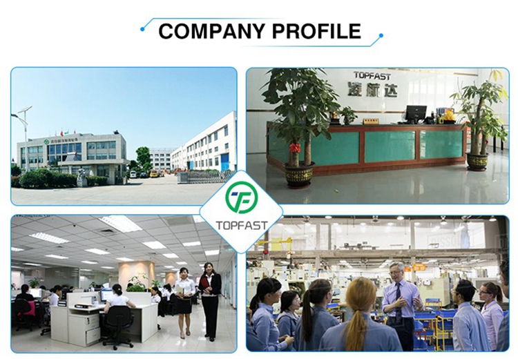
Topfast is a manufacturer that focus on PCB,PCBA manufacturing over 20 years.We have an excellent r&d team of 28 people.We can help you with one-stop service. To support you with the whole process from function research and development, product PCB design discussion, PCB manufacturing, component procurement to PCB assembly.
Our company providing PCB industry solutions for customers in the field of templates and small volumes.With high quality and on time delivery product, we won the market's wide acclaim. We will continue to focus on customer satisfaction, along with "high quality"and "fast delivery", the company will become an electronic circuit service provider worthy of customer trust.Our factory mainly produces ordinary double-sided PCB, multi-layer boards pcb, HDI pcb boards, metal based pcb board, ceramic pcb.semiconductor pcb boards, rigid-flex pcb boards and flexible pcb boards.
PCB EXHIBITION
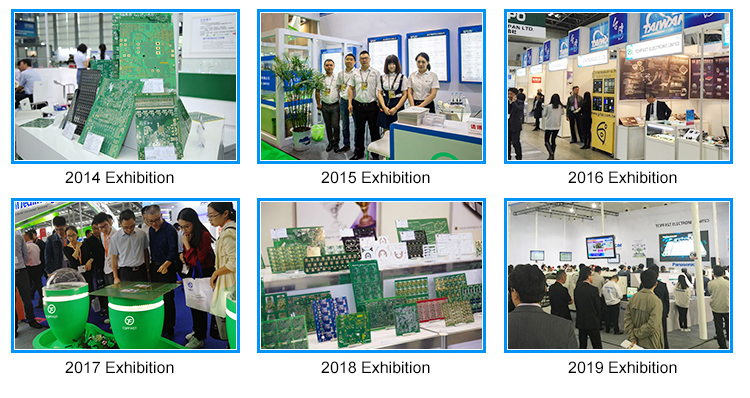
TopFast’s annual internation pcb exhibiton attracts old and new customers from Europe ,America ,Asia ,Oceana and so on .
During their visit ,they highly appraise our products and priase our customer-centered ,continuous innovation ,win-win cooperation spirit.
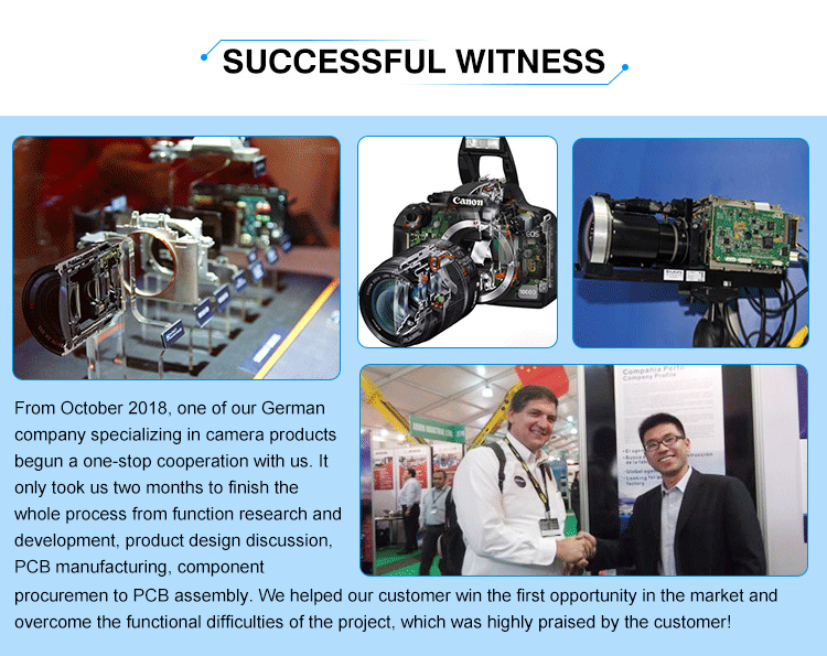
From October 2018.one of our Germancompany specializing in camera productsbegun a one-stop cooperation with us.
ltonly took us two months to finish the whole process from function research anddevelopment. product design discussion,
PCB manufacturing. component procuremen to PCB assembly. We helped our customer win the first opportunity in the market
andovercome the functional difficulties of the pcb pcba project, which was highly praised by the customer!
PCB certification
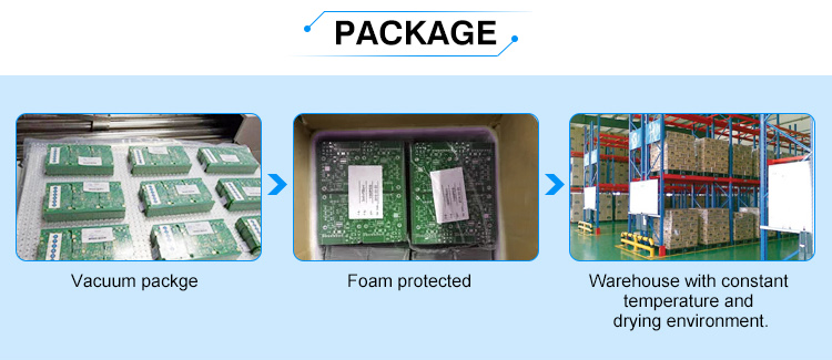
Our pcb and pcba with vacuum package,with safety and professional shipping.


Q1:What kind of PCB file format can you accept for production?
Gerber, PROTEL 99SE, PROTEL DXP, CAM350, ODB+(.TGZ)
Q2:Is my PCB files safe when I submit them to you for manufacturing?
We respect customer's copyright and will never manufacture PCB for someone else with your files unless we receive written permission from you, nor we'll share these files with any other 3rd parties.
Q3:What payments do you accept ?
-Wire Transfer(T/T),Western Union,Letter of Credit(L/C)
-Paypal ,Ali Pay,Credit Cart
Q4:How to get the PCBs?
A:For small packages, we will ship the boards to you by DHL,UPS,FedEx,EMS. Door to door service! You will get your PCBs at your home.
B:For heavy goods more than 300kg, we may ship your boards by ship or by air to save freight cost. Of course, if you have your own forwarder, we may contact them for dealing with your shipment.
Q5:What is your minimum order quantity?
Our MOQ is 1 PCS.
Q6: Can we visit your company?
No problem. You are welcome to visit us in Shenzhen. Or the other factory is in GuangDong province.
Q7: How can you ensure the quality of the PCBs?
Our PCBs are 100% test including Flying Probe Test, E-test and AOI.
Address of Plant
PCB Factory:
A1 Building, B Zone, Ditang Industrial Zone, Ditang Road, Shajing Street, Bao'an District, Shenzhen, China
PCBA Factory:
Room 805, Room 806, Room 809, No. 96, Chuangqiang Road, Ningxi Street, Zengcheng District, Guangzhou City, Guangdong Province, P.R. China
Office Address:
Room 805, Room 806, Room 809, No. 96, Chuangqiang Road, Ningxi Street, Zengcheng District, Guangzhou City, Guangdong Province, P.R. China