
Precision PCB Solutions for High-Demand Applications
Since 2008, Topfast has been committed to delivering high-quality PCB manufacturing and assembly services worldwide. We offer end-to-end solutions spanning from precision manufacturing to comprehensive functional testing, ensuring accuracy and reliability at every stage.
Specializing in rapid prototyping and turnkey assembly services, we leverage our technical expertise and proven execution capability to provide efficient, integrated, and trustworthy solutions for all your PCB needs.
- Full Turnkey PCBA Services
- Premium PCB Fabrication
- Reliable SMT Assembly
- Authentic Component Sourcing
- Rigorous Quality Control
Why Choose Topfast PCB
Your Success From Our Close Collaboration.
Complete Manufacturing Solutions
From rapid prototyping to mass production, we ensure consistent product quality through expert manufacturability support and engineering consulting.
Trusted Partner
Our ISO-certified facilities, rigorous testing processes, competitive pricing, and efficient delivery cycles collectively guarantee your project's success from concept to market.
0
Daily Orders
0
SQM Factory
0
Global Partners
0
Technology Patents
Why Topfast?
PCB/PCBA Service
One-Stop PCBA Services
Up to 64-layer PCB manufacturing
Global Parts Procurement
BOM Cost Optimization
Cost Reduction and Efficiency Enhancement
Quick Turnaround

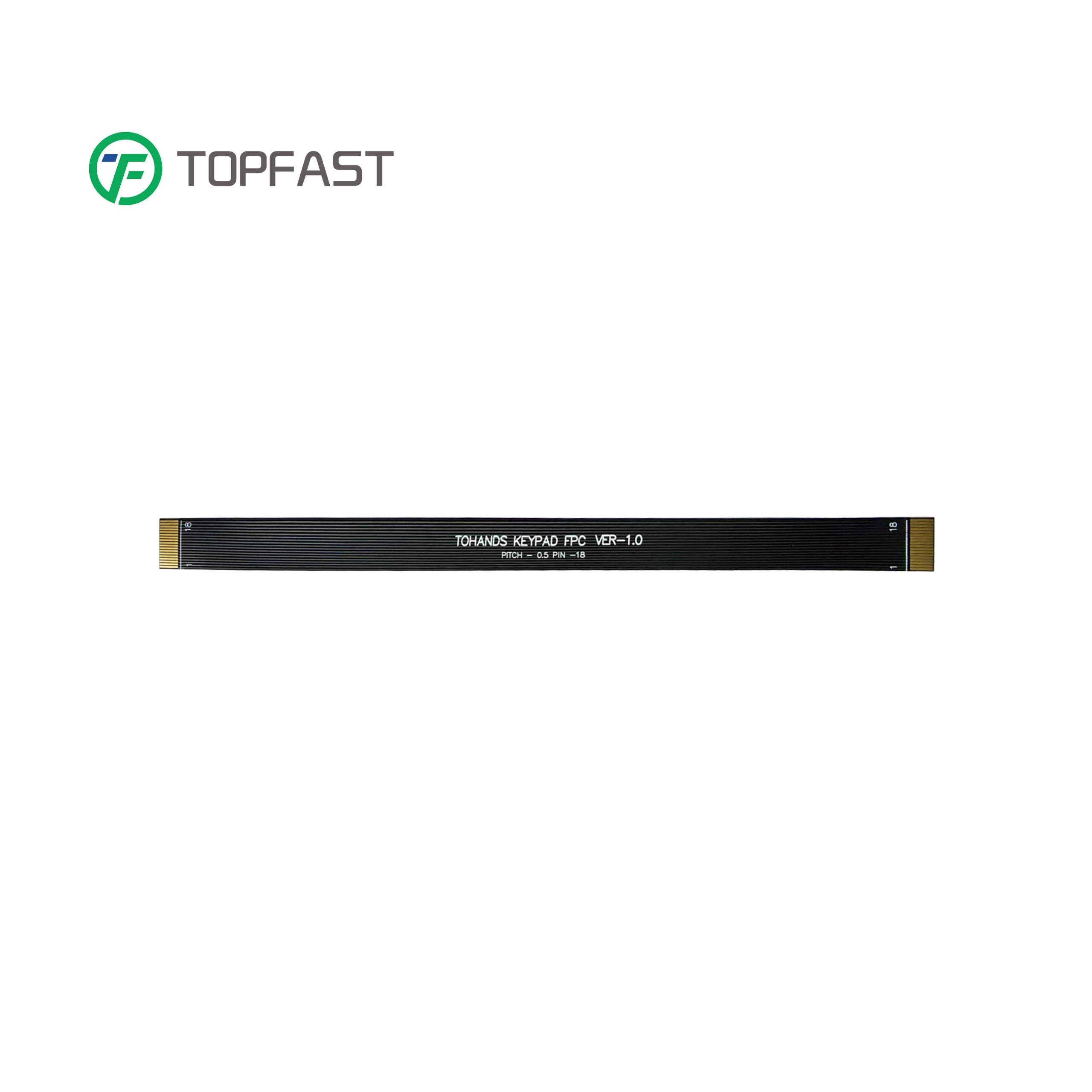
Wire Harness Service
Custom Cable Assembly
Custom Wire Harness
10,000 SQM ISO Certified Factory
High Capacity Manufacturing
10+ Industries Served
Professional Customization
Topfast Capabilities
Line Width/Space
1.8mil/1.8mil
Blind and Buried Vias
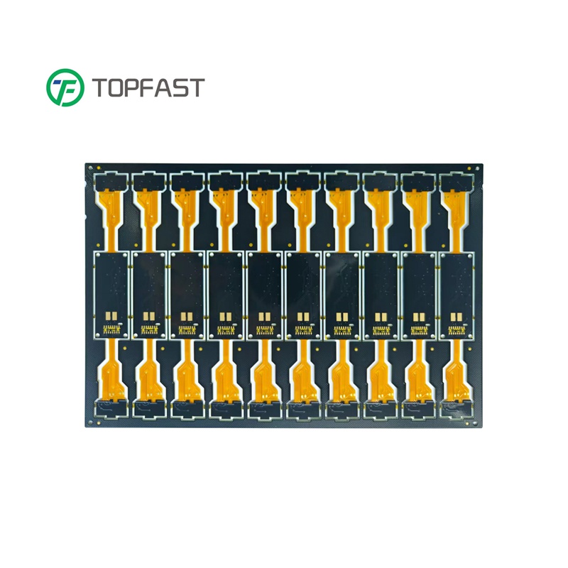
Rigid, Flex, Rigid-Flex
Size Down to 0201
RoHS Compliant
Thickness 0.1mm to 12mm
IPC A 610H
Controlled Impedance
Double Side BGA
X-Ray Inspection
Lead Free, HASL, OSP etc
Min Hole Dia. to 0.1mm
CNC / Metals
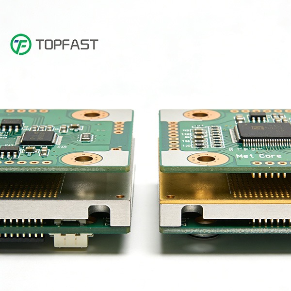
Turnkey Assembly
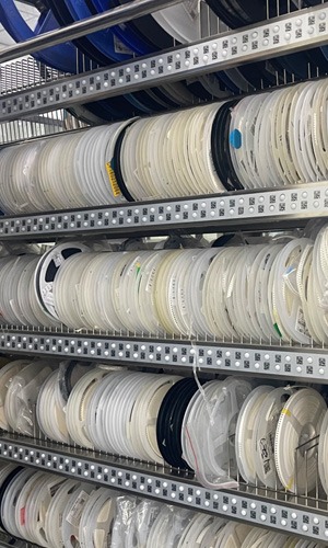
Components Sourcing
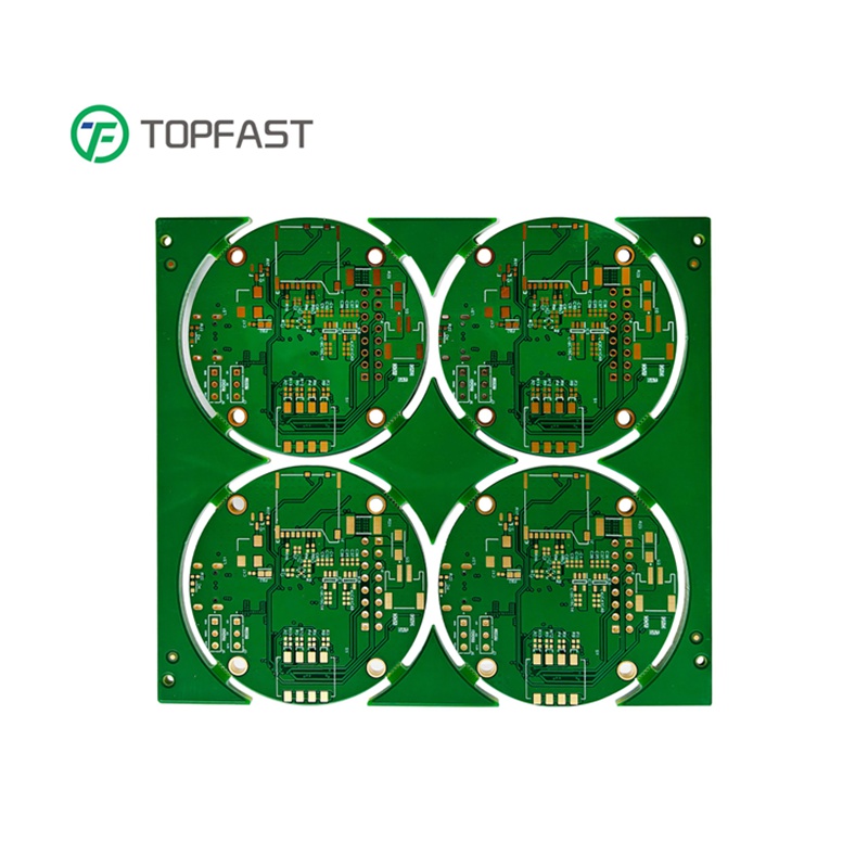
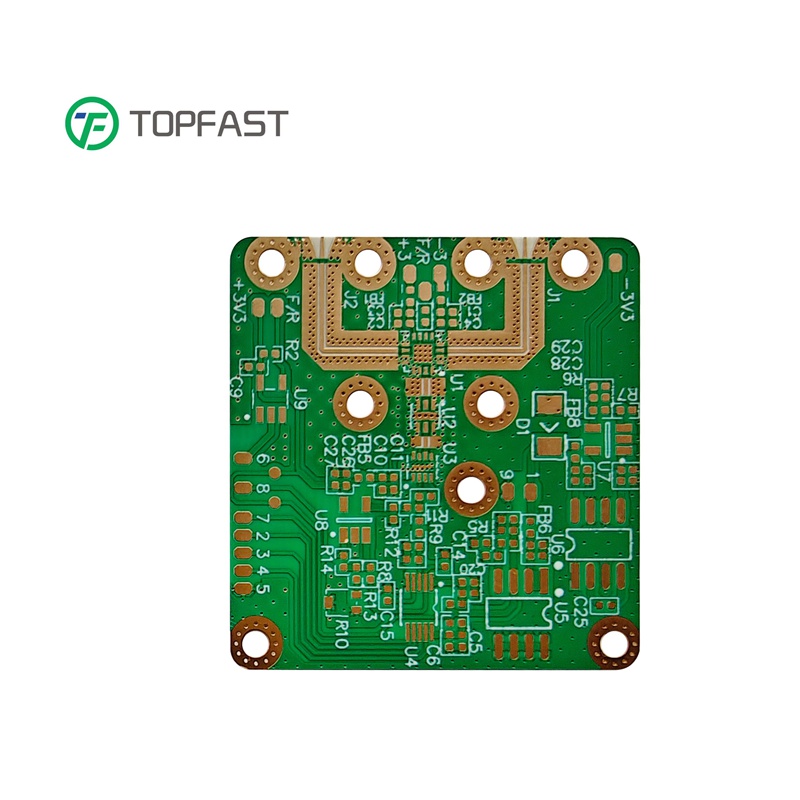


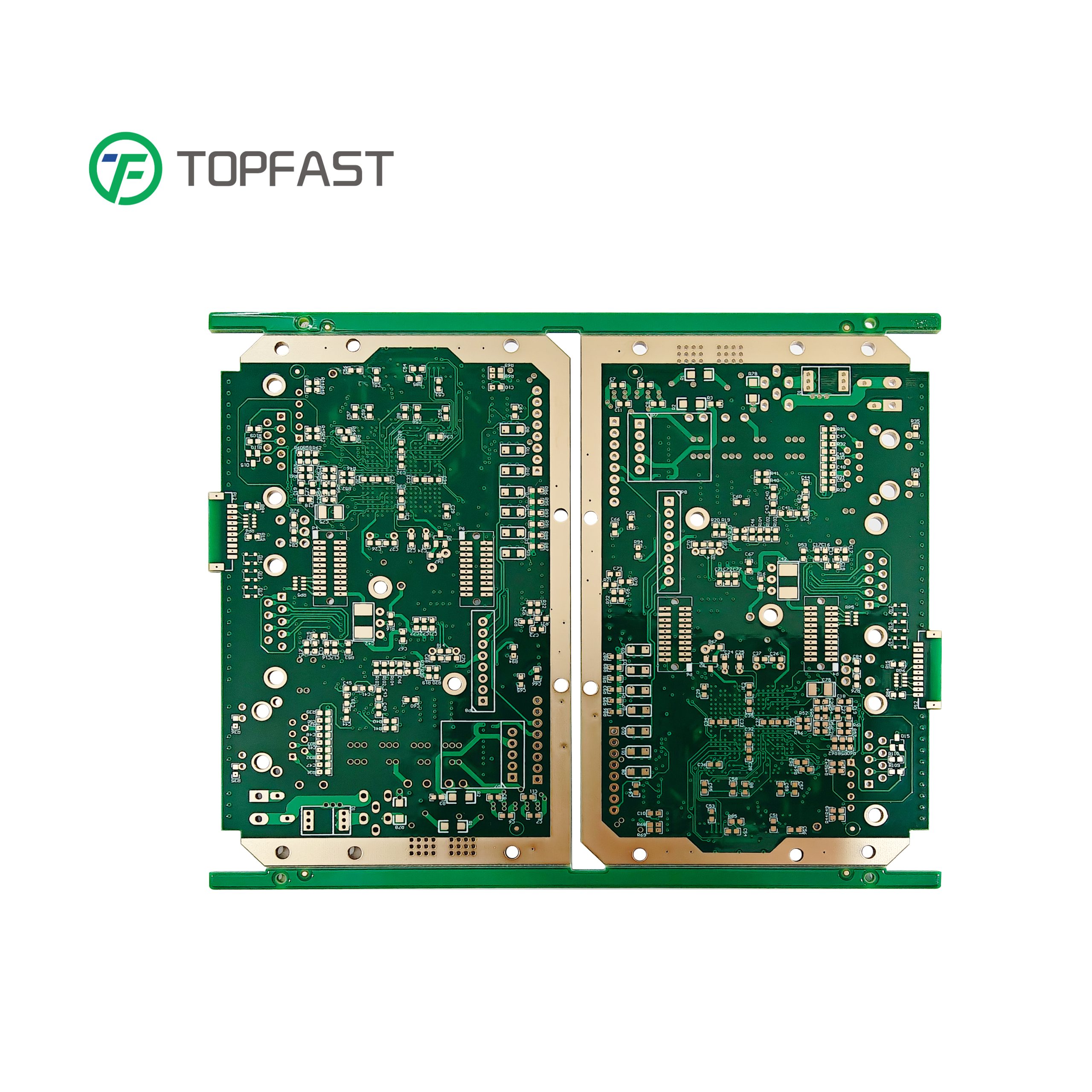
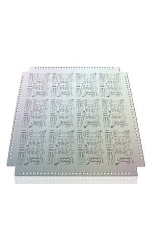
Multilayer PCB Capabilities
Precision multilayer PCB manufacturing from standard 4-layer boards to ultra-complex high-layer-count HDI structures.
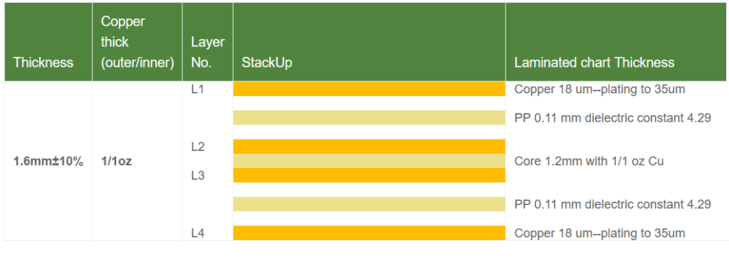
4 Layer PCB
Cost-effective multilayer solution ideal for consumer electronics, IoT products, and embedded systems.
- Signal-GND-PWR-Signal stack-up
- Better EMI control than 2-layer PCB
- Compact routing structure
6 Layer PCB
Balanced performance for industrial control systems, automotive ECUs, and mixed-signal applications.
- Improved signal isolation
- Enhanced grounding performance
- Stable power distribution
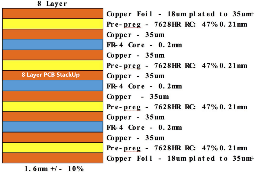
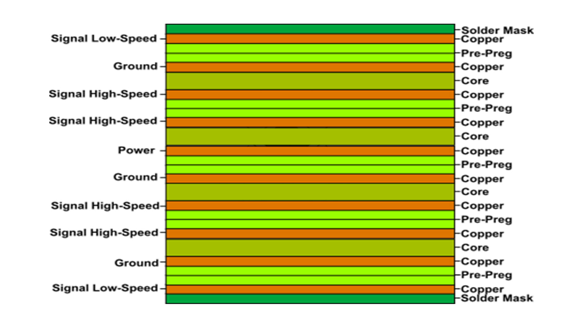
8 Layer PCB
Optimized for networking equipment, DDR memory routing, and telecom infrastructure systems.
- Multiple reference planes
- DDR3 / DDR4 compatible
- Better SI & EMI performance
10 Layer PCB
Designed for demanding applications requiring controlled impedance and high-density routing capability.
- Controlled impedance design
- Advanced EMI suppression
- High-reliability stack-up
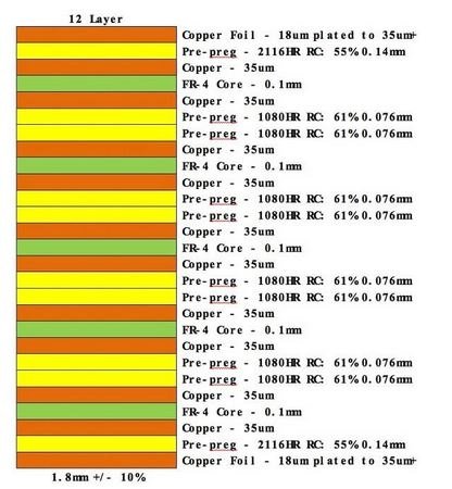
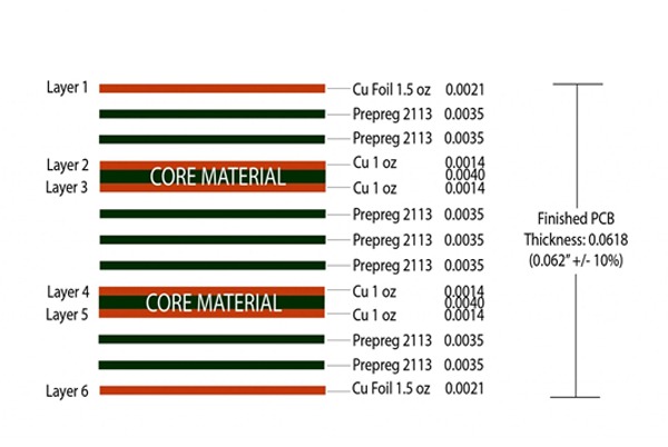
12 Layer PCB
Sequential lamination and HDI technology for servers, storage, and telecom backplanes.
- HDI structure support
- 25Gbps+ signal routing
- High routing density
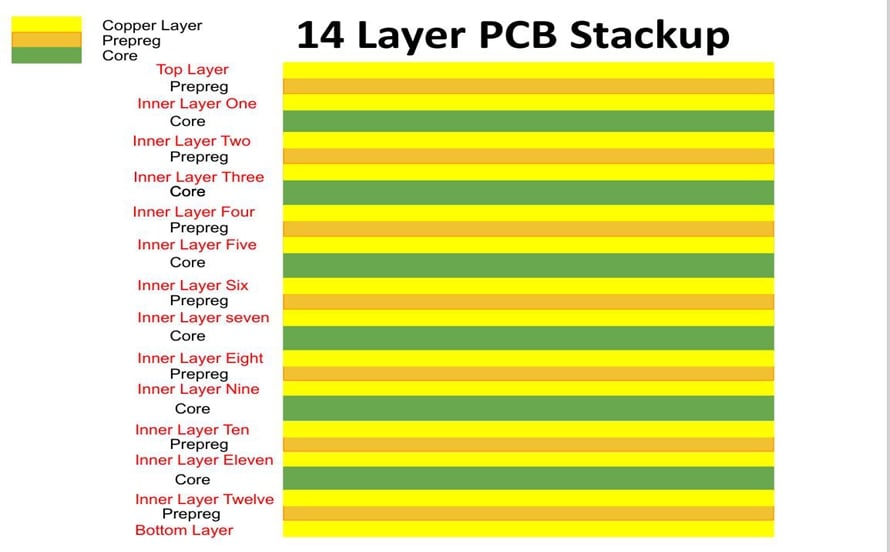
14 Layer PCB
Ultra-complex routing architecture supporting multiple voltage domains and high-speed backdrill structures.
- Backdrill compatible
- Via-in-pad technology
- Extreme signal integrity
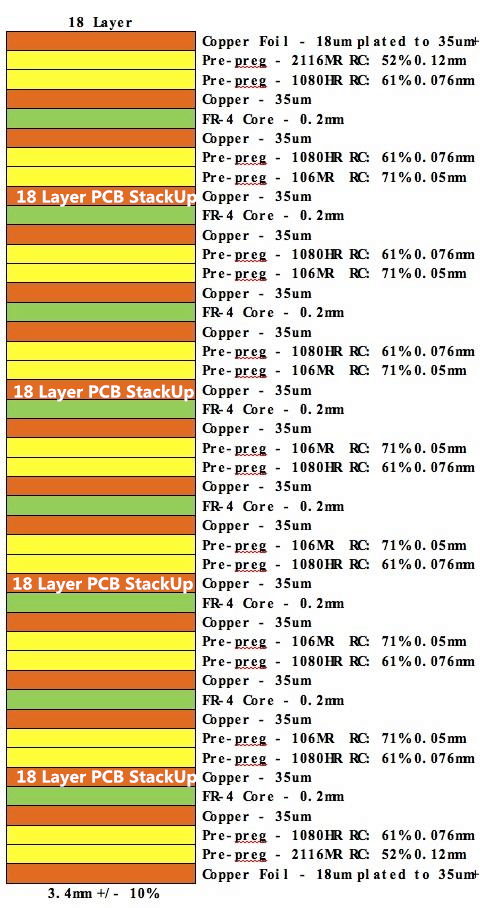
14+ Layers PCB
Custom high-layer-count PCB solutions for AI computing, military systems, data centers, and advanced networking.
- Up to 64-layer capability
- Sequential lamination
- Ultra-low-loss materials
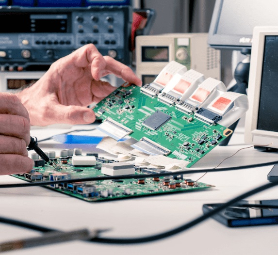
PCB Assembly Manufacturer
Advanced Technology for Precision Electronics Manufacturing
IQC Warehouse
Incoming Quality Control ensures all components meet our strict standards before assembly.
SMD Stencils
Precision stencils for accurate solder paste application in surface mount technology.
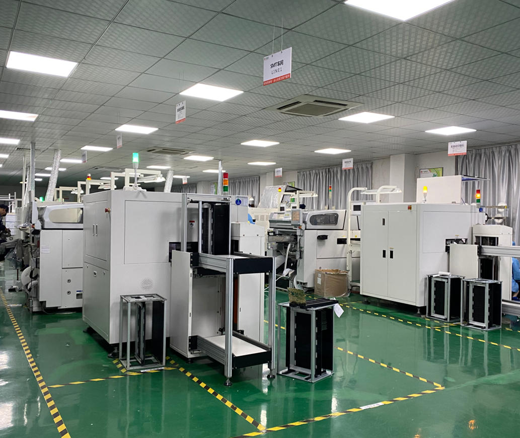
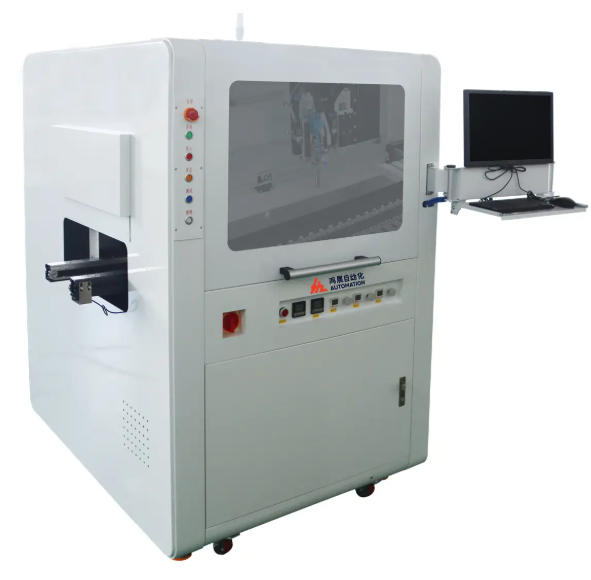
SMT Line 1 & 2
State-of-the-art surface mount technology lines for high-volume production with precision.
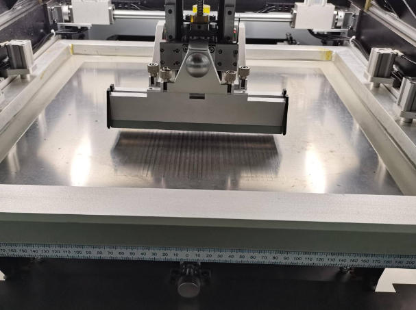
Solder Paste Printing Machine
Advanced printing technology for precise solder paste application on PCBs.
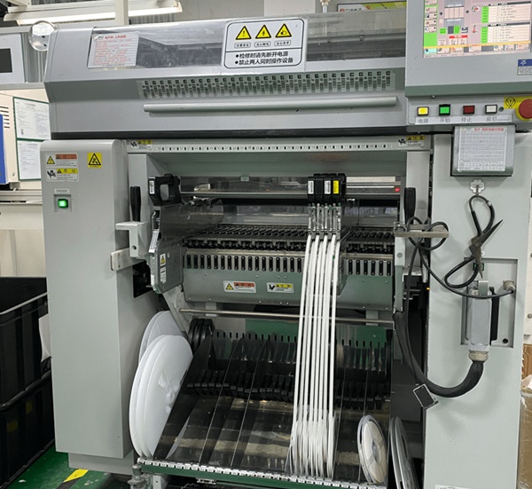
Pick and Place Machine
High-speed automated component placement with Yamaha precision technology.
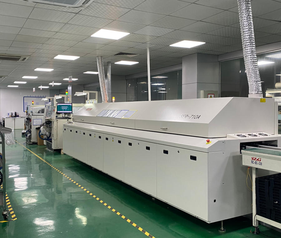
Reflow Oven
Precision temperature profiling for perfect solder reflow in surface mount assembly.
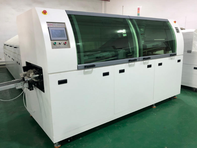
Wave Soldering Machine
Advanced wave soldering technology for through-hole component assembly.
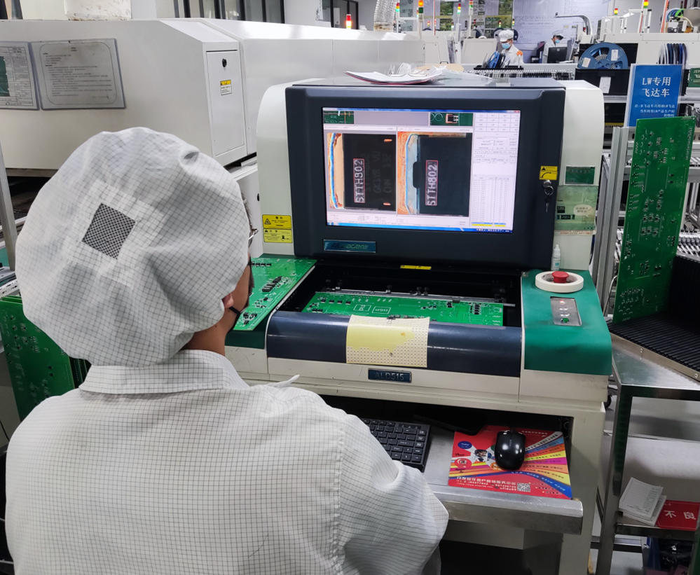
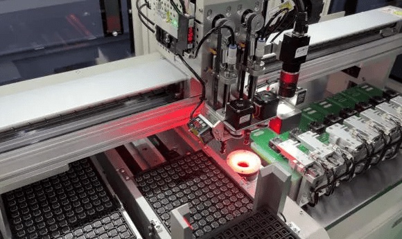
AOI Inspection
Automated Optical Inspection for detecting assembly defects and quality assurance.
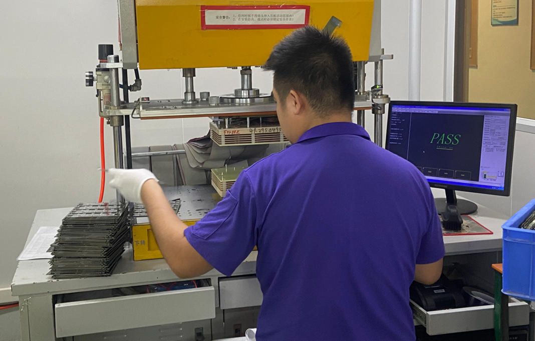
Quality Control Inspection
Rigorous quality control processes to ensure every PCB meets the highest standards.
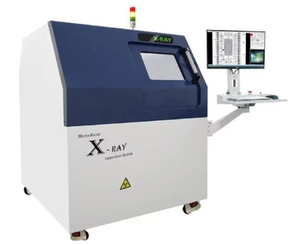
X-ray Inspection
Non-destructive testing for detecting hidden defects in BGA and complex assemblies.
PCBA Dry Ice Cleaning
Eco-friendly dry ice cleaning technology for removing contaminants from assembled boards.
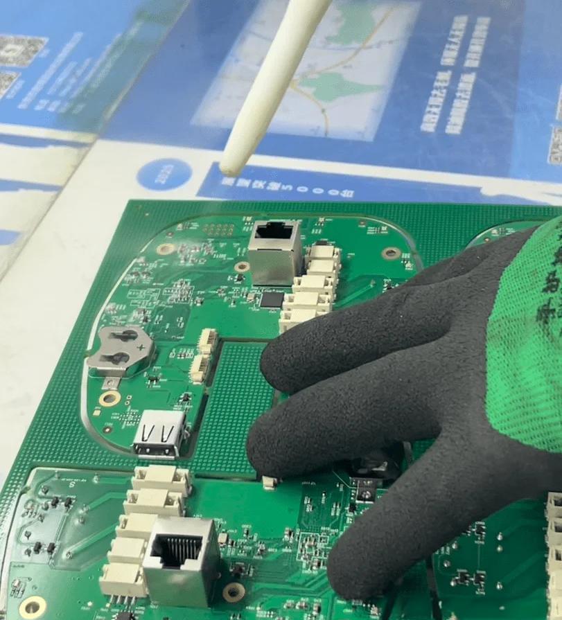
PCBA Functional Testing
Comprehensive functional testing to ensure assembled boards operate as designed.
IC Programming & Testing
Programming and validation of integrated circuits for fully functional assemblies.
Conformal Coating Machine
Automated application of protective coatings for enhanced durability and reliability.
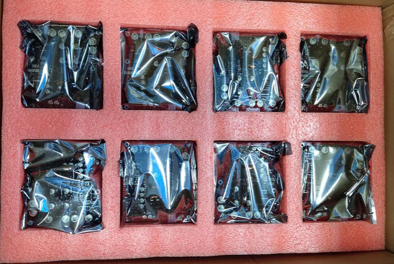
PCBA Packaging
Secure and professional packaging solutions to protect finished assemblies during shipping.
PCB Order Process
PCB Testing ServicesWe perform 100% full inspection on every circuit board. Through advanced methods including flying probe testing, AOI automatic optical inspection, X-ray inspection, ICT in-circuit testing, and test racks, we comprehensively detect open circuits, short circuits, and electrical performance issues in PCBs. With the most stringent quality control processes, we ensure every product delivers reliable quality and stable performance.
PCBA Testing Services We utilize YAMAHA high-speed pick-and-place machines and
an intelligent material storage system to achieve high-precision SMT assembly. Throughout
production, advanced equipment including SPI, AOI, X-RAY, and functional test fixtures
comprehensively ensure quality
SPI: Automatically inspects solder paste thickness, area, and placement to enhance
soldering quality and efficiency.
AOI: Precisely identifies component soldering status, positional deviations, and missing
parts.
X-RAY: Performs X-ray inspection of internal structures, focusing on complex components
like BGAs.
Test Fixtures: Load firmware and commands to comprehensively validate PCBA functional
reliability.
We rigorously execute every process step, committed to delivering premium products and
dependable services to our customers.
Our Certifications
All our PCB products are IPC rated and have UL, ROHS and ISO9001 certifications, ensuring the highest quality standards.

Quality Management System
GB/T19001
Automotive Quality System
IATF16949
Quality Management System
ISO9001
Environmental Management System
ISO14001
Safety Certification
ULClient Reviews
Hear what our clients have to say about our services and quality
Communication was seamless throughout the entire process. The Topfast team was very responsive and attentive to my specific requirements. They patiently listened to my project needs, offering valuable suggestions and recommendations to optimize the design and functionality of my PCBs.

Intel
R&D Manager
When I received my circuit boards, I was amazed at the quality of them. The boards were clearly made with precision and attention to detail, and everything was exactly as I had specified in my order. The silkscreened labels were crisp and clear, all the components fit perfectly, and the result exceeded our expectations.

Samsung
Electronics Engineer
I recently had the pleasure of working with Topfast, a leading PCB prototype manufacturer, and I must say that my experience was simply outstanding. From start to finish, their service and product quality exceeded my expectations and I am happy to share my positive feedback.

Panasonic
Product Designer
Your Trusted PCB Manufacturer & Wiring Harness Provider
Get A Quote
High-Quality PCB Manufacturing,
Assembly & Wiring Harness Services
Fast Turnaround & Reliable Service
