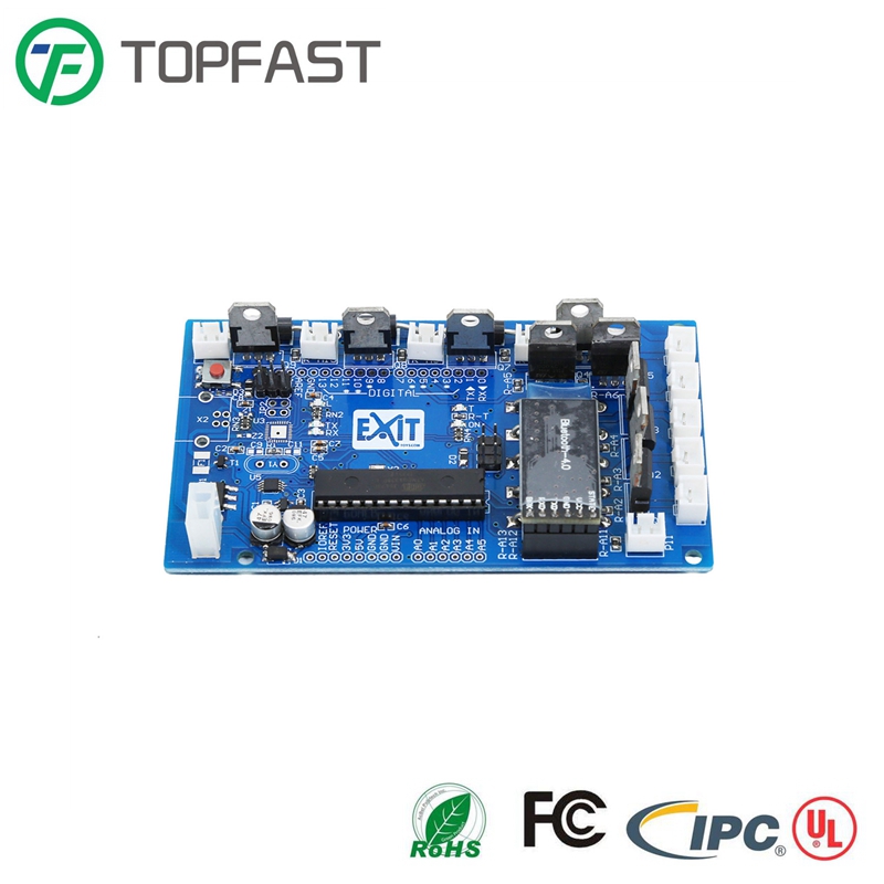
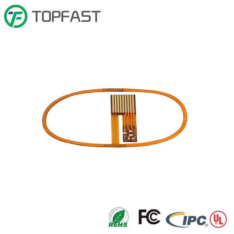
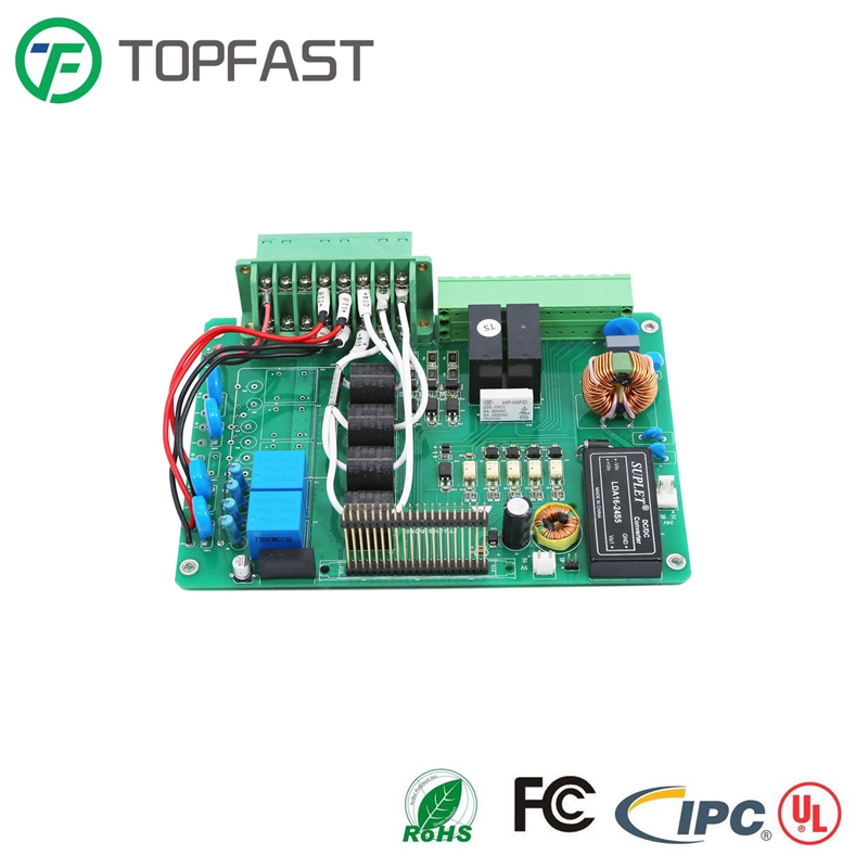
The printed circuit board assembly process is not complete until a reliable inspection process is completed. Its ability to point out hidden defects cannot be overemphasized. It can save you valuable time and protect you from costly mistakes later, and rightfully so.
The following are some common PCB inspection processes that are often performed.
Manual PCB Inspection
As the name implies, it involves manually looking at components to check them for problems.
AOI PCB Inspection
Automatic or automated optical inspection involves using an optical system to take images of PCB components and identify any defects.
AXI PCB Inspection
As the PCB density increases, not all solder joints are visible. Therefore, optical inspection may not serve the purpose. In this case, the X-ray system - AXI is able to look under the chip to see the solder joints.
X-ray Inspection: X-ray inspection is ideal for more complex boards and offers features that other inspection methods cannot. X-ray inspection allows you to see inside solder joints to find bubbles that cannot be seen with AOI.

Let's look at some of the defects that can be easily pointed out using these PCB inspection techniques.
The use of through-holes in PCBs has become ubiquitous because they help to easily connect different layers of the board. However, the integrity of blind and buried holes cannot be determined by visual inspection. x-ray inspection, although it can send radiation that can penetrate hidden spots, can easily assess the quality of connections and components.
The landing pattern of a specific element on a board will usually have errors associated with it. For example, if the board is using elements that are not included in the common SMD component library, the likelihood of a landing pattern error is much higher.
By using a ball grid array system, components are packaged at high density on the board. In this case, a PCB X-ray can also come in handy to check the quality of the components and board connections. the images generated by the PCB X-ray are very helpful in looking at individual components and identifying any defects.

Decoupling capacitors help ensure power supply stability as well as eliminate oscillations and transients. However, incorrect capacitor placement can lead to poor device performance. The inspection process ensures that any misplacement can be easily identified and corrected.
Soldering plays a very important role in attaching components to the board. Any errors in soldering can lead to faulty connections and can affect the integrity of the PCB.
Therefore, inspections must be performed to look for solder voids that could lead to low quality connections. In turn, it ensures that low-quality connections can be avoided.
Through-hole is an important technique for connecting components to the PCB. However, it is prone to a number of defects, including pinhole filling. Essentially, they occur due to the escape of gases during soldering. If too much heat is applied to the solder, this can lead to continuous gas escape. Pinhole filling can be identified and the integrity of the solder determined during quality assessment.

PCB inspection offers a wide range of benefits and ensures quality control of the PCB. In fact, inspecting PCBs helps to improve the entire PCB production process. If a particular defect tends to recur, you can correct that defect at the process level itself. From this perspective, PCB inspection plays an important role in the continuous improvement of the PCB production process. If you are looking for a reliable PCB manufacturer, please contact TOPFAST.
Address of Plant
PCB Factory:
A1 Building, B Zone, Ditang Industrial Zone, Ditang Road, Shajing Street, Bao'an District, Shenzhen, China
PCBA Factory:
4/F, Building 21, No. 46 Xinye Road, Yonghe Development Zone, Huangpu District, Guangzhou, China
Office Address:
Room 2201-03 & 2206, Building 1, Changfeng International, No. 96, Li Xin 12 Road, Zengcheng District, Guangzhou City, Guangdong Province, China.