What is smt ?
SMT stands for Surface Mount Technology, which is a method used in the assembly of printed circuit boards (PCBs). It is a widely used technology in the electronics industry for mounting electronic components onto PCBs.
In SMT, electronic components are mounted directly onto the surface of the PCB, as opposed to through-hole technology (THT) where components have leads that are inserted into holes on the PCB and soldered on the other side. SMT components are typically smaller and lighter, allowing for higher component density on the PCB.
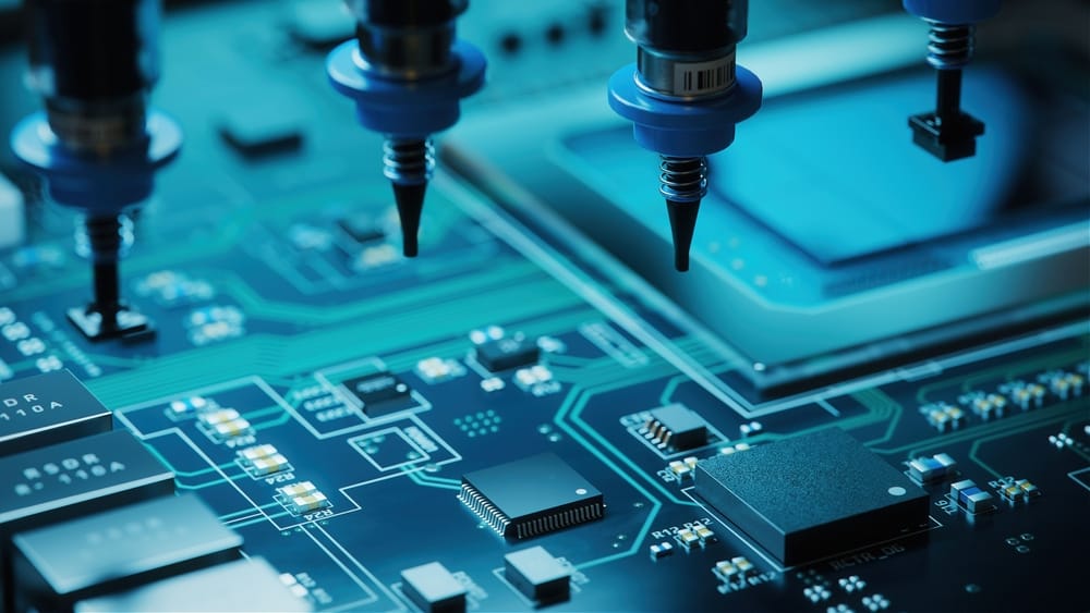
1. Component Placement: Automated machines, known as pick-and-place machines, accurately place the surface mount components onto the PCB. These machines use vision systems to align the components with the correct orientation and position.
2. Solder Paste Application: A stencil is used to apply solder paste onto the PCB, which is a sticky mixture of solder and flux. The solder paste is applied to the pads on the PCB where the components will be placed.
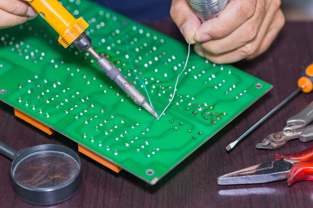
3. Reflow Soldering: The PCB with the components and solder paste is passed through a reflow oven. The oven heats the PCB to a specific temperature, causing the solder paste to melt and create a bond between the components and the PCB. The solder solidifies as the PCB cools down, creating a permanent connection.

What is the SMT used for?
SMT (Surface Mount Technology) PCB is used for the assembly of electronic components onto printed circuit boards (PCBs). It is a widely adopted technology in the electronics industry and is used for various applications. Here are some common uses of SMT:
Consumer Electronics: SMT is extensively used in consumer electronic devices such as smartphones, tablets, laptops, televisions, gaming consoles, and audio/video equipment. The compact size and high component density achieved through SMT enable the miniaturization of these devices.
Automotive Electronics: SMT is employed in automotive electronics for applications like engine control units (ECUs), infotainment systems, advanced driver-assistance systems (ADAS), sensors, and lighting systems. SMT allows for smaller and more reliable electronic components in vehicles.
Industrial Electronics: SMT is utilized in industrial electronic equipment such as control systems, robotics, factory automation, power supplies, and instrumentation. The high component density and improved performance achieved through SMT are beneficial in industrial applications.
Medical Devices: SMT is used in medical devices like patient monitoring systems, diagnostic equipment, imaging devices, and implantable devices. The small form factor and high precision of SMT components are advantageous in medical applications.
Aerospace and Defense: SMT is employed in aerospace and defense electronics for applications like avionics systems, communication equipment, radar systems, navigation systems, and military-grade electronics. SMT enables lightweight and compact designs for these critical applications.
Telecommunications: SMT is widely used in telecommunications equipment such as routers, switches, modems, base stations, and network infrastructure. The high-speed and high-frequency capabilities of SMT components are essential for efficient data transmission.
IoT (Internet of Things): SMT plays a crucial role in IoT devices, including smart home devices, wearables, connected sensors, and other IoT-enabled products. SMT allows for small, power-efficient, and interconnected components in IoT applications.
Overall, SMT is used in a wide range of industries and applications where compact size, high component density, improved performance, and reliability are essential. It enables the production of smaller, lighter, and more advanced electronic devices with enhanced functionality.
The PCB STM assembly process:
The PCB SMT (Surface Mount Technology) assembly process involves several steps to assemble electronic components onto a printed circuit board (PCB). Here is a detailed overview of the PCB SMT assembly process:
Stencil Printing: A stencil is aligned with the PCB, and solder paste is applied to the solder pads using a squeegee. The stencil has openings corresponding to the component footprints on the PCB. The solder paste is a mixture of solder alloy and flux.
Component Placement: Automated pick-and-place machines accurately place the surface mount components onto the solder paste on the PCB. These machines use vision systems to identify the correct component orientation and position. The components are picked from reels, trays, or tubes and precisely placed onto the solder pads.
Reflow Soldering: The PCB with the components and solder paste is passed through a reflow oven. The oven has multiple heating zones that gradually raise the temperature. The solder paste melts, creating a bond between the component leads and the solder pads on the PCB. As the PCB moves through the oven, it reaches a peak temperature where the solder reflows and forms reliable solder joints. The PCB then exits the oven and cools down, solidifying the solder joints.
Inspection: After reflow soldering, the PCB undergoes inspection processes to check for any defects. Automated Optical Inspection (AOI) systems or X-ray machines are used to inspect the solder joints, component placement, and overall quality. Any defects or issues are identified for further analysis and correction.
Cleaning (optional): Depending on the application and requirements, the assembled PCB may undergo a cleaning process to remove any flux residues or contaminants left from the soldering process. This step is particularly important for high-reliability applications.
Testing: The assembled PCB may undergo functional testing to ensure it meets the required specifications. This can include electrical testing, functional testing, or programming of components if necessary.
Additional Assembly Steps: After SMT assembly, the PCB may undergo further assembly processes, such as through-hole component insertion, wave soldering, conformal coating, or final testing, depending on the specific requirements of the product.

The advantages of SMT Assembly :
Surface Mount Technology (SMT) offers several advantages over traditional through-hole technology (THT) in the assembly of electronic components onto printed circuit boards (PCBs). Here are some key advantages of SMT:
Size and Weight Reduction: SMT components are smaller and lighter compared to their through-hole counterparts. This allows for higher component density on the PCB, enabling the design and production of smaller and more compact electronic devices.
Increased Component Density: SMT allows for closer placement of components on the PCB, resulting in higher component density. This leads to more functionality in a smaller space, making it ideal for applications where size is a constraint.
Improved Electrical Performance: SMT components have shorter electrical paths and reduced lead lengths, resulting in lower parasitic capacitance and inductance. This leads to improved signal integrity, reduced signal delays, and better overall electrical performance of the circuit.
Enhanced High-Frequency Performance: SMT components are better suited for high-frequency applications due to their reduced lead lengths and improved electrical characteristics. They exhibit lower parasitic effects, making them suitable for applications such as telecommunications, wireless communication, and high-speed data transmission.
Cost Efficiency: SMT assembly processes can be highly automated, leading to increased efficiency and productivity. The automated pick-and-place machines used in SMT assembly reduce labor costs and improve production throughput. Additionally, SMT components are often less expensive than their through-hole counterparts.
Improved Thermal Performance: SMT components have a smaller footprint and better thermal conductivity, allowing for efficient heat dissipation. This is particularly important for power electronics and devices that generate significant heat during operation.
Design Flexibility: SMT offers greater design flexibility as it allows for more complex and intricate PCB layouts. The smaller size of SMT components enables designers to create innovative and space-saving designs, accommodating various functionalities on a single PCB.
Automated Inspection and Testing: SMT assembly processes can be easily integrated with automated inspection systems, such as Automated Optical Inspection (AOI) and X-ray machines. These systems can quickly and accurately inspect solder joints, component placement, and overall quality, ensuring higher reliability and reducing the chances of defects.
Overall, SMT provides numerous advantages in terms of size reduction, increased component density, improved electrical and thermal performance, cost efficiency, design flexibility, and automated inspection. These advantages make SMT the preferred choice for modern electronic assembly, enabling the production of smaller, lighter, and more advanced electronic devices.
Address of Plant
PCB Factory:
A1 Building, B Zone, Ditang Industrial Zone, Ditang Road, Shajing Street, Bao'an District, Shenzhen, China
PCBA Factory:
4/F, Building 21, No. 46 Xinye Road, Yonghe Development Zone, Huangpu District, Guangzhou, China
Office Address:
Room 2201-03 & 2206, Building 1, Changfeng International, No. 96, Li Xin 12 Road, Zengcheng District, Guangzhou City, Guangdong Province, China.