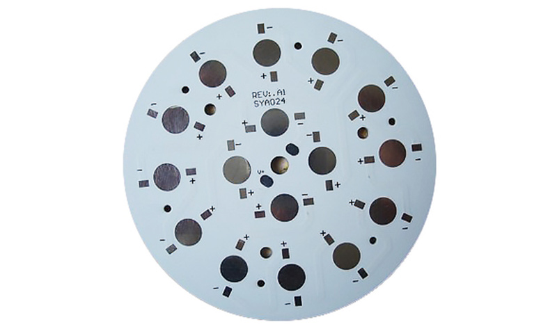
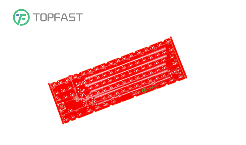
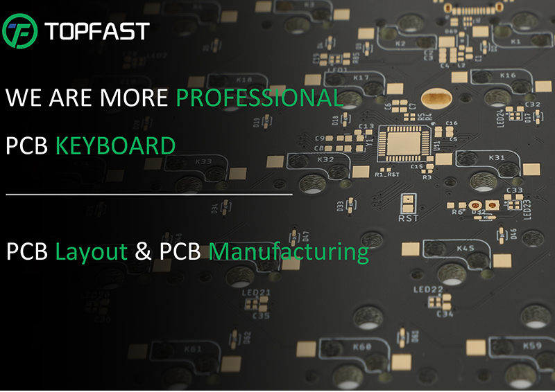
A bare PCB is a printed circuit board without solder resist layers, it has only one or two circuit layers so PCB designers can cut or solder copper traces to test their designs. Printed plate manufacturer TOPFAST explains what it is used for and what we can do for you.

To understand bare PCB, you should know the difference between bare PCB and bare PCB.
A bare PCB is an incomplete circuit board with no solder resist covering the copper traces, and a bare PCB is a complete circuit board with no mounted components. Depending on the need, you can print on bare PCB with or without screen printing. And bare PCBs also have PCB pads.
After generating the electrical traces on the PCB core or laminate, the surface finish (e.g. OSP, ENIG) is applied to the PCB pads and then screen printed on the laminate material.
In our experience, the demand for bare PCBs is not that great. Customers who order bare PCBs have not yet defined their project design and they use bare PCBs to test their design on the board.
The copper traces of the bare PCB are exposed and engineers can easily cut and solder the traces. After the engineers have finalized their project design, they can contact us to fabricate and assemble the PCBs.
The use of bare PCBs still occurs during the project development phase, when the PCB design is almost complete.

Bare PCBs allow for more complex circuit designs at a lower cost.
Unlike design testing of PCB prototypes, there are no solder resist layers on bare PCBs and it is easy to cut or solder copper wires. And bare PCBs are far less expensive to manufacture than PCB prototypes.
Bare PCBs are printed circuit boards, while breadboards are not. The effect of circuit testing on them is different, and bare PCBs to a large extent perform almost identically to the final product.
Modifying and testing your design with bare PCBs provides more assurance for the final product. Bare PCBs are easy to debug, and using them to modify your design before PCB manufacturing can avoid possible financial losses.
Feel free to continue to be prepared to consult us when you have modified the PCB and decided to manufacture and assemble the board using electronic components. You can enjoy these benefits.
High-quality PCB manufacturing that meets IPC ratings and is UL, ROHS and ISO9001 certified
24-hour technical hotline, any time you want to stay in touch with our CAM engineers
Complete PCBA samples and PCBA functional testing for large orders
Quality-traceable, no-profit electronic component procurement services
All orders receive a free engineering file review before proceeding to manufacturing

Bare PCBs have no solder resist layer and the copper traces are exposed. This makes it easy to cut and solder wires, and in this way, engineers can use bare PCBs to modify your designs. Please send us a message to learn more and get working together soon.
Address of Plant
PCB Factory:
A1 Building, B Zone, Ditang Industrial Zone, Ditang Road, Shajing Street, Bao'an District, Shenzhen, China
PCBA Factory:
Room 805, Room 806, Room 809, No. 96, Chuangqiang Road, Ningxi Street, Zengcheng District, Guangzhou City, Guangdong Province, P.R. China
Office Address:
Room 805, Room 806, Room 809, No. 96, Chuangqiang Road, Ningxi Street, Zengcheng District, Guangzhou City, Guangdong Province, P.R. China