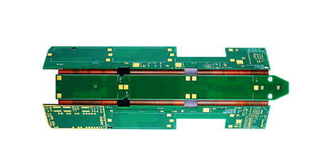
Due to the large number of layers in the multilayer PCB board, the user has
higher and higher requirements for calibration of the PCB layer. Typically, the
alignment tolerance between layers is controlled at 75 microns. So do you know
the difficulties of China Multilayer PCB Board? Let us study together.

1. Difficulties in the production of internal circuit.
The multilayer pcb board adopts special materials such as high TG, high speed, high frequency, thick copper and thin dielectric layer, which puts high requirements on internal circuit fabrication and graphic size control. For example, the integrity of impedance signal transmission increases the difficulty of internal circuit fabrication.
The width and line spacing are small, the open circuit and short circuit increase, the short circuit increases, the pass rate is low; the thin line signal layer is more, the inner layer AOI leakage detection probability increases; the inner core board is thin, easy to wrinkle, poor exposure, easy to curl when etching machine; The high-level plate is mostly a system board, the unit size is large, and the product scrapping cost is high.
2. Difficulties in compression manufacturing.
Many inner and pre-cured sheets are superimposed, which are prone to defects such as sliding, delamination, resin voids and bubble residue in stamping production. In the design of the laminated structure, the heat resistance, pressure resistance, rubber content and dielectric thickness of the material should be fully considered, and a reasonable multi-layer circuit board material pressing scheme should be formulated.
3. Difficulties in drilling.
The use of high TG, high speed, high frequency, thick copper special plates increases the difficulty of drilling roughness, drilling burrs and drilling. The number of layers is large, the total copper thickness and plate thickness are accumulated, the drill is easy to break the knife; the dense BGA is more, the CAF failure problem caused by the narrow hole wall spacing; the plate thickness is easy to cause the oblique drilling problem.
If you also have any other difficulties, please contact us 18 Layers Rigid PCB Board Exporter, who can give you a professional guide.
Address of Plant
PCB Factory:
A1 Building, B Zone, Ditang Industrial Zone, Ditang Road, Shajing Street, Bao'an District, Shenzhen, China
PCBA Factory:
4/F, Building 21, No. 46 Xinye Road, Yonghe Development Zone, Huangpu District, Guangzhou, China
Office Address:
Room 2201-03 & 2206, Building 1, Changfeng International, No. 96, Li Xin 12 Road, Zengcheng District, Guangzhou City, Guangdong Province, China.