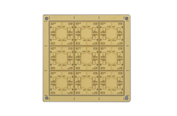
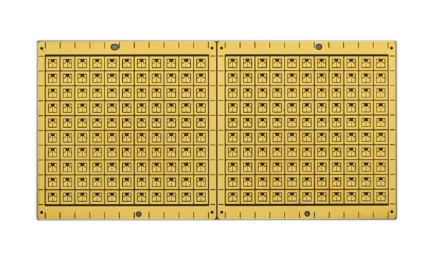
Many experts consider ceramic PCBs to be more advantageous than traditional FR4 PCBs. Although ceramic PCBs are relatively new in the list of PCB substrates, they are becoming increasingly popular for use in high-density electronic circuits. Ceramic PCBs have high thermal conductivity and coefficient of thermal expansion. These PCBs are best suited for high power density circuit designs used in extreme conditions, especially in the aerospace and automotive industries.

As you know, ceramics have more advantages over MCPCBs, such as high operating temperature, high thermal conductivity, good insulation and thermal properties that can make a difference to the material. More importantly, ceramic PCBs have efficient thermal conductivity.
Ceramic PCBs can only be seen in products with big performance, while they are not available in ordinary products. As a result, ceramics are replacing entire printed circuit boards to reduce manufacturing and design complexity and improve performance.
Ceramic PCBs are undoubtedly the best solution to overcome thermal cycling failures due to their high thermal conductivity, stability and inertness, and because they also have CTE compatible with leading ceramic chip carriers and characteristics. Ceramic PCB practice is divided into three catalogs: high temperature co-fired ceramic PCB, thick film ceramic PCB and low temperature co-fired ceramic PCB.
First, it can use silver or gold conductive paste in the ceramic PCB manufacturing process to place traces connected in each layer. In general, metal components or substrates are placed in each layer using a layer-by-layer screen printing process. In addition, it is possible to mechanically punch holes in the unfired layers or drill microvias with a laser.
Next, after printing and stacking the ceramic layers, it bakes the entire stack in an oven. In general, the firing temperature required to fire ceramic PCBs is below 1000°C, which matches the firing temperature of gold and silver pastes. So the low temperature baking process is the reason for allowing gold or silver in ceramic PCBs.
However, the hot pressing/baking and sintering process for multilayer PCBs allows for the immediate integration of passive components into the inner layers of ceramic PCBs with ease. This is not possible in boards made of FR-4 material, so PCB designers can increase the component and connection density of the inner layers.
Ceramic PCBs are now widely used due to their high thermal conductivity, low CTE, low dielectric constant and chemical resistance.
For example, a Japanese company used a multilayer ceramic PCB containing four IC chips to manufacture a 1Mbit SRAM memory module, which helped achieve high reliability and high-density assembly. In addition, a U.S. company has used ceramic PCBs to manufacture missiles, telecom products and aerospace products. Their common feature is that they can be used in extreme environments. The multi-layer ceramic PCBs and packaging components provide sufficient strength and resistance to shock and vibration at the warhead.
One U.S. company makes radar receive/transmit modules from ceramic PCBs. The high thermal conductivity and low CTE of aluminum nitride provide a good basis for the use of ceramic PCBs in receive/transmit modules.

Deep ultraviolet Food Preservation Pcb
Ceramic PCB in the same PCB area of the number of components more to accommodate the miniaturization of electronic products, ceramic PCB in the application of multilayer interconnect board more possibilities.
What's more, a Japanese company uses LTCC PCBs to manufacture analog/digital PCBs, thereby reducing parasitic capacitance by about nine-tenths. It not only effectively overcomes crosstalk interference in circuit tracking, but also reduces the size and weight of the circuit.
Please contact TOPFAST if you have any questions!
Address of Plant
PCB Factory:
A1 Building, B Zone, Ditang Industrial Zone, Ditang Road, Shajing Street, Bao'an District, Shenzhen, China
PCBA Factory:
4/F, Building 21, No. 46 Xinye Road, Yonghe Development Zone, Huangpu District, Guangzhou, China
Office Address:
Room 2201-03 & 2206, Building 1, Changfeng International, No. 96, Li Xin 12 Road, Zengcheng District, Guangzhou City, Guangdong Province, China.