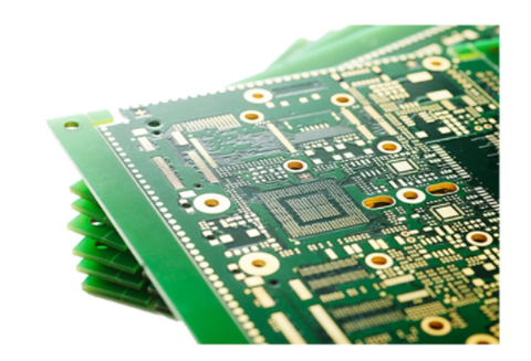
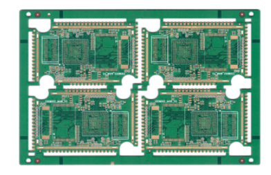
High Density Interconnect (HDI) PCBs are the most popular type of printed circuit board and are widely used in a variety of compact, high-performance electronic devices. As electronic devices and their components become smaller, these printed circuit boards pack more circuitry and functionality into a smaller area.
Although HDI PCBs appear to be compact, it involves details and several complex elements which add to the cost. This article provides tips on how to reduce the cost of HDI PCBs without sacrificing quality and performance.
The cost of an HDI PCB can be influenced by several factors. Addressing these factors and choosing the right alternative will help you save on PCB manufacturing costs and optimize the value of your PCB investment.

Stacking is one of the significant features that increase the cost of PCB assembly. 1-n-1, 2-n-2, and 3-n-3 are the most common types of HDI stacking. 2-n-2 layouts are considered more challenging than 1-n-1, and 3-n-3 is even more challenging than 2-n-2. This is because as the number of layers increases, so does the workload.
Through-hole is the term for the electrical connection established between two layers of a PCB. A through-hole has two pads that are adjacent to each other on two different layers of the board. Micro-through-holes are small through-holes with a hole diameter of 0.15 mm. They are usually drilled using laser equipment and require high precision. Microvia holes can increase your costs. Therefore, it is always wise to choose the through-hole type keeping in mind the application requirements.
This is also one of the important pricing factors. The conductive or non-conductive hole filling process depends on the design. Some designs require vias underneath surface mount components that need to be filled, capped or plated. The fill process often requires multiple plating and drilling steps, which can require additional time and effort.

Stacked vias are typically filled with copper, while staggered vias are not. No additional imaging steps are required in staggered vias. However, stacked vias require planarization as well as additional imaging steps. All of this makes staggered vias very simple compared to stacked vias. The simplicity helps to further reduce manufacturing costs.
Glass fiber, FR4 and copper are a few popular core materials used to build HDI PCBs. These materials have different physical properties and therefore they cost differently. When selecting materials, it is important to focus on three properties - the material's dimensional stability, processability, and ability to withstand multiple layers of lamination. HDI designs involve laser drilling, and problems may arise if the material cannot withstand drilling. Therefore, it is important to ensure that the material meets all of these requirements while providing price advantages.
Since the functionality of electronic devices depends on these PCBs, it is important to design and manufacture them from a trusted manufacturer. TOPFAST is one such experienced manufacturer that specializes in custom PCBs. we have been customizing a variety of PCBs to our customers for commercial, industrial and mission critical applications. Contact us for a quote!
Address of Plant
PCB Factory:
A1 Building, B Zone, Ditang Industrial Zone, Ditang Road, Shajing Street, Bao'an District, Shenzhen, China
PCBA Factory:
4/F, Building 21, No. 46 Xinye Road, Yonghe Development Zone, Huangpu District, Guangzhou, China
Office Address:
Room 2201-03 & 2206, Building 1, Changfeng International, No. 96, Li Xin 12 Road, Zengcheng District, Guangzhou City, Guangdong Province, China.