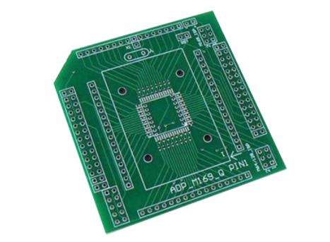
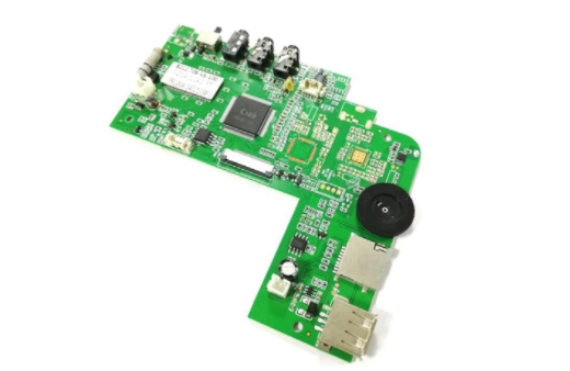
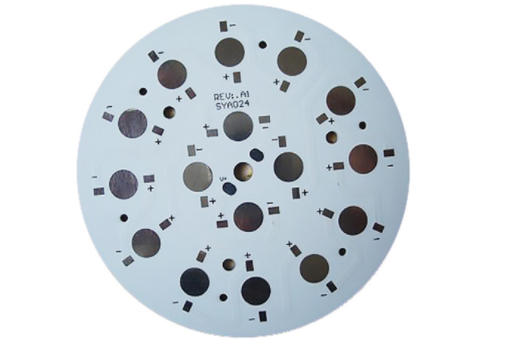
For electronic equipment, the work will generate a certain amount of heat, so that the internal temperature of the device rises rapidly, if the heat is not distributed in a timely manner, the device will continue to heat up, the device will fail due to overheating, the reliability of electronic equipment performance will be reduced.
Therefore, it is very important to have a good heat dissipation process for the PCB board. Let's discuss this together.
Heat dissipation through the PCB board itself is widely used PCB board is a copper / epoxy glass cloth substrate or phenolic resin glass cloth substrate, and a small number of paper-based copper laminate used.
Although these substrates have excellent electrical properties and processing performance, but poor heat dissipation, with electronic products have entered the miniaturization of components, high-density installation, high heat generation assembly era, if only rely on the surface area of very small components to dissipate heat is very insufficient.

Heat sensitive devices are placed in the cold air area. Temperature detecting devices are placed in the hottest locations.
The devices on the same printed board should be arranged as much as possible according to their heat generation and the degree of heat dissipation partition, heat generation is small or heat-resistant devices placed in the uppermost stream of the cooling airflow (entrance), heat generation or heat-resistant devices (such as power transistors, large-scale integrated circuits, etc.) placed in the most downstream of the cooling airflow.
Devices that are more sensitive to temperature are best placed in the lowest temperature area (such as the bottom of the device), never place it directly above the heat-generating devices, and multiple devices are best laid out staggered on a horizontal plane.
The devices with the highest power consumption and the greatest heat generation are arranged near the best location for heat dissipation. Do not place devices with higher heat generation in the corners and around the edges of the printed board, unless a heat sink is arranged near it. Choose larger devices when designing power resistors and adjust the layout of the board so that there is enough space for heat dissipation.
For more info about PCB assembly, please contact us.

High heat-generating devices plus heat sink, thermal conductivity board when there are a few devices in the PCB when the heat generation is large (less than 3), you can add heat sink or thermal conductivity tube on the heat-generating devices, when the temperature can not be lowered, you can use a heat sink with a fan to enhance the cooling effect.
When the amount of heat-generating devices is more (more than 3), a large heat sink cover (board) can be used, which is customized according to the location and height of the heat-generating devices on the PCB board and a special heat sink or a large flat heat sink keyed to different component height positions. The heat sink is snapped onto the component surface as a whole, contacting each component and dissipating heat.

Heat dissipation is achieved by using a reasonable alignment design. The heat dissipation of the printed circuit board in the device mainly relies on air flow, so the air flow path should be studied during the design and the device or printed circuit board should be reasonably configured.
Air flow always tends to flow where there is less resistance, so when configuring devices on the printed circuit board, avoid leaving a large open area in a certain area. The same attention should be paid to the configuration of multiple printed circuit boards in the whole machine.
If there are conditions, the thermal efficiency of the printed circuit analysis is necessary, such as some professional PCB design software now adds the thermal efficiency index analysis software module can help designers optimize circuit design. So please get in touch with TOPFAST, we offer custom solutions for you.
Address of Plant
PCB Factory:
A1 Building, B Zone, Ditang Industrial Zone, Ditang Road, Shajing Street, Bao'an District, Shenzhen, China
PCBA Factory:
4/F, Building 21, No. 46 Xinye Road, Yonghe Development Zone, Huangpu District, Guangzhou, China
Office Address:
Room 2201-03 & 2206, Building 1, Changfeng International, No. 96, Li Xin 12 Road, Zengcheng District, Guangzhou City, Guangdong Province, China.