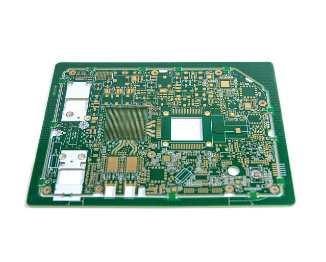
PCB is short for printed circuit board (Printed Circuit Board), which is the support body of electronic components, but also the carrier of the electrical connection of electronic components. PCB design needs to be achieved with the help of computer-aided design, the industry's common design software: Cadence Allegro, PADS, Altium Designer, etc..
Conventional PCB design includes several steps such as library building, netlist transfer, layout, wiring, file output, etc., but the conventional PCB design process is far from being able to meet the increasingly complex high-speed PCB design requirements. The actual PCB design process is much more complex.
On the basis of comprehensive consideration of signal quality, EMC, thermal design, DFM, DFT, structure, safety requirements, etc., the devices are placed on the board in a reasonable manner - PCB layout.
The layout should try to meet the following requirements: the total connection is as short as possible, with the shortest key signal lines; high voltage and high current signals are completely separated from the weak signals of low voltage and small current signals; analog signals are separated from digital signals; high frequency signals are separated from low frequency signals; and the spacing of high frequency components should be adequate. Local adjustments are made under the premise of meeting the requirements of simulation and timing analysis.

Realize the design of physical connection between device pins under the requirement of following the rules of signal quality, DFM, EMC, etc. --Wiring
PCB wiring design is the largest workload in the entire PCB design process, which directly affects the performance of the PCB board. Some of the basic requirements for wiring processing are as follows.
(1) over-hole, line width, safety spacing to avoid the use of extreme values.
(2) the distance from the alignment to the edge of the board is usually required ≥ 2mm, in the case of failure to meet the conditions, at least ensure that not less than 20mil.
(3) metal housing devices under the device, do not allow over-hole, surface alignment.
(4) Try to provide a dedicated wiring layer for clock signals, high-frequency signals, sensitive signals and other critical signals, and to ensure that its minimum loop area. Use shielding and increase the safety spacing and other methods to ensure signal quality.
5) The EMC environment between the power supply layer and the ground layer is poor, and the arrangement of signal lines sensitive to interference should be avoided.
(6) Wiring as close as possible to a plane and avoid cross-segmentation. If it is necessary to cross the division or cannot be close to the power ground plane, these situations are only allowed to exist in the low-speed signal lines.
(7) plane layer and wiring layer distribution symmetry, media thickness distribution symmetry, across the hole across the layer to maintain symmetry.
(8) All signal lines must be chamfered, chamfer angle of 45 degrees, except in special cases.
Even if the wiring in the entire PCB board is completed well, the interference caused by poorly considered power and ground lines can degrade the performance of the product, and sometimes even affect the success of the product. Therefore, the treatment of power and ground should be taken seriously to minimize the noise and interference generated by the power and ground to ensure the quality of the product.
(1) try to widen the width of the power and ground lines, preferably wider than the power lines, their relationship is: ground - power lines - signal lines.
(2) the PCB of the digital circuit can be wide ground wire to form a circuit, that is, to form a ground network to use (analog circuit ground can not be used in this way)
(3) with a large area of copper layer for the ground, the printed board is not used in the place are connected to the ground as a ground. Or multilayer board, power and ground each occupy a layer.
After the wiring design is completed, it is necessary to carefully check whether the wiring design conforms to the rules set by the designer, and also to confirm whether the rules set meet the production process requirements of the printed board.
1) Whether the distance between line and line, line and component pad, line and hole, component pad and hole, and hole and hole is reasonable and meets the production requirements.
(2) whether the width of the power and ground lines are appropriate, whether the coupling between the power and ground, and whether there are still places in the PCB where the ground line can be widened.
(3) whether the best measures are taken for key signal lines (such as the shortest length, add protection lines, input and output lines are clearly separated)
(4) whether the analog and digital circuit parts have their own separate ground.
(5) whether the graphics (such as icons, labeling) added later in the PCB will cause a signal short circuit.
(6) whether the process line is added to the PCB, whether the solder resist meets the requirements of the production process, whether the size of the solder resist is appropriate, whether the character markings pressure device pads.

TOPFAST is a professional PCB supplier. We committed to offering the highest quality pcb design at the most competitive pricing. Our platform has the best credibility in Google. We have advanced equipment and professional technical team can ensure a quality product in a timely manner. Please feel free to contact us if you need any help, our experts will help you with your solutions.
tel: +86 17702089421
email: sales@topfastpcb.com
Address of Plant
PCB Factory:
A1 Building, B Zone, Ditang Industrial Zone, Ditang Road, Shajing Street, Bao'an District, Shenzhen, China
PCBA Factory:
Room 805, Room 806, Room 809, No. 96, Chuangqiang Road, Ningxi Street, Zengcheng District, Guangzhou City, Guangdong Province, P.R. China
Office Address:
Room 805, Room 806, Room 809, No. 96, Chuangqiang Road, Ningxi Street, Zengcheng District, Guangzhou City, Guangdong Province, P.R. China