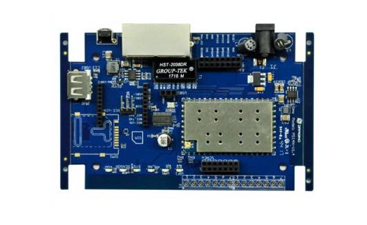
The basic characteristics of the printed circuit board depending on the performance of the substrate board. To improve the technical performance of the printed circuit board, the performance of the printed circuit board must be improved first. In order to meet the needs of the development of the printed board, various new materials It is being gradually developed and put into use.
Embedded Components PCB Manufacturer talked about the recent shift in the focus of the PCB market from computers to communications, including base stations, servers, and mobile terminals. Mobile communication devices represented by smartphones have driven the development of PCBs towards higher density, thinner and higher functions. Printed circuit technology is inseparable from the substrate material, which also involves the technical requirements of the substrate for PCB. Now the relevant content of the substrate material is organized into a special article for reference by the CCL industry.
Communication PCB Wholesalers pointed out the demand for high-density thin wires. PCBs are all developing to high-density thin wires, and HDI boards are particularly prominent. Ten years ago, the definition of IPC for HDI board was that the line width/line spacing (L / S) was 0.1mm / 0.1mm and below, and now the industry basically achieves a conventional L / S of 60μm and an advanced L / S 40μm. Japan ’s 2013 version of the installation technology roadmap data is that the 2014 HDI board conventional L / S is 50 μm, the advanced L / S is 35 μm, and the trial-production L / S is 20 μm.

Medical Equipment PCBA
PCB circuit pattern formation, the traditional is the chemical etching process (subtraction method) after photo-imaging on the copper foil substrate, the limit of the subtraction method for making fine circuits is about 30μm, and a thin copper foil (9 ~ 12μm) substrate is required. Due to the high price of thin copper foil CCL and many defects in thin copper foil lamination, many factories produce 18μm copper foil and then use etching to reduce the copper layer in production. This method has many processes, difficult thickness control, and high cost. It is still better to use thin copper foil. In addition, when the L / S of the PCB circuit is less than 20 μm, the general thin copper foil is also inadequate. An ultra-thin copper foil (3 to 5 μm) substrate and an ultra-thin copper foil attached to the carrier are required.
Demand for laminated dielectric sheets. The technical characteristic of HDI board is the buildup process (BuildingUpProcess), the commonly used resin coated copper foil (RCC), or the laminate of semi-cured epoxy glass cloth and copper foil is difficult to achieve fine lines. Now tend to use semi-additive method (SAP) or modified semi-processing method (MSAP), that is, using an insulating dielectric film layer, and then electroless copper plating to form a copper conductor layer, because the copper layer is very thin and easy to form fine lines.
One of the key points of the semi-additive method is the laminated dielectric material. In order to meet the requirements of high-density thin lines, the dielectric material, electrical insulation, heat resistance, bonding strength and other requirements are proposed for the laminated material, and the adaptability to the HDI board process. At present, the international HDI laminated media materials are mainly ABF / GX series products of Japan Ajinomoto Co., which uses epoxy resins and different curing agents to add inorganic powder to increase the rigidity of the material and reduce CTE. Glass fiber cloth is also used to enhance the rigidity . There is also a similar film laminate material from Japan Sekisui Chemical Co., Ltd., which has also been developed by the Taiwan Institute of Technology. ABF materials are also constantly improving and developing. The new generation of laminated materials particularly require low roughness, low thermal expansion rate, low dielectric loss and thin rigidity.
High heat dissipation requirements
With the miniaturization and high function of electronic equipment, which generate high heat generation, the thermal management requirements of electronic equipment continue to increase. One solution chosen is the development of thermally conductive printed circuit boards. The primary condition for heat-resistant and heat-dissipating PCBs is the heat resistance and heat dissipation of the substrate. At present, the heat resistance and heat dissipation of the substrate are improved to a certain extent through resin improvement and filler addition, but the improvement of thermal conductivity is very limited. Typically, a metal substrate (IMS) or metal core printed circuit board is used, which plays a role in heat dissipation of heat-generating components, which reduces the size and cost of cooling compared with traditional radiators and fans.
If you are interested, please contact our Rigid PCB Manufacturer.
Address of Plant
PCB Factory:
A1 Building, B Zone, Ditang Industrial Zone, Ditang Road, Shajing Street, Bao'an District, Shenzhen, China
PCBA Factory:
4/F, Building 21, No. 46 Xinye Road, Yonghe Development Zone, Huangpu District, Guangzhou, China
Office Address:
Room 2201-03 & 2206, Building 1, Changfeng International, No. 96, Li Xin 12 Road, Zengcheng District, Guangzhou City, Guangdong Province, China.