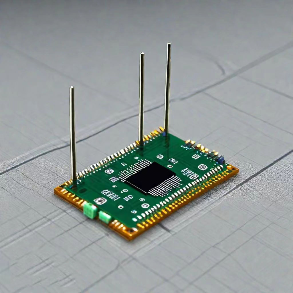
1 Preferred surface mount and crimp components
Surface assembly components and crimped components have good manufacturability.
With the development of component packaging technology, the vast majority of components can be purchased in packaging categories suitable for reflow soldering,
including plug-in components that can use through-hole reflow soldering. If the design can realize full-surface assembly, the efficiency and quality of assembly will be
greatly improved.
Crimped components are mainly multi-pin connectors, and this type of package also has good manufacturability and connection reliability, which is also the preferred
category.

2 Shorten the process path
The shorter the process path, the higher the production efficiency and the more reliable the quality, the preferred process path design is:
single-sided reflow soldering;
double-sided reflow soldering;
Double-sided reflow soldering + wave soldering;
Double-sided reflow soldering + selective wave soldering;
Double-sided reflow soldering + manual soldering.
3 Optimize component layout
Component layout design mainly refers to the layout orientation and spacing design of components. The layout of the components must meet the requirements of the
welding process. Scientific and reasonable layout can reduce the use of bad solder joints and tooling, and can optimize the design of steel mesh.

4 The overall consideration of the design of pads, solder masks and stencil fenestration is considered
The design of pads, solder masks and stencil fenestration determines the actual amount of solder paste and the formation of solder joints. Coordinating the design of
pads, solder masks and stencils plays a very important role in improving the first-pass rate of welding.

5 Focus on new packages
The so-called new packaging does not necessarily refer to the new packaging on the market, but refers to those packaging that your company has no experience in using.
For the introduction of new packages, process validation of small batches should be performed. The premise of use must be to have done experiments, understand the process
characteristics and problem spectrum, and master the countermeasures.

6 Focus on BGAs, chip capacitors, and crystal oscillators
BGA, chip capacitors and crystal oscillators are typical stress-sensitive components, and should be placed in places where PCBs are prone to bending and deformation during
welding, assembly, workshop turnover, transportation, and use.

7 Study case studies to refine design rules
Design for manufacturability rules are derived from production practice, and it is of great significance to continuously optimize and improve design rules according to the
continuous cases of assembly defects or failures.
Address of Plant
PCB Factory:
A1 Building, B Zone, Ditang Industrial Zone, Ditang Road, Shajing Street, Bao'an District, Shenzhen, China
PCBA Factory:
4/F, Building 21, No. 46 Xinye Road, Yonghe Development Zone, Huangpu District, Guangzhou, China
Office Address:
Room 2201-03 & 2206, Building 1, Changfeng International, No. 96, Li Xin 12 Road, Zengcheng District, Guangzhou City, Guangdong Province, China.